Semiconductor in numbers: Asian water infrastructure buildout
Share this insight
This chart shows major water utility projects and investments for Asia’s semiconductor manufacturing sites. Unlike in the US, where utilities are often expanded reactively around specific projects, Asian infrastructure is typically planned upfront at the science park or regional level, with strong government coordination.
This results in large, shared systems, including reclaimed water networks, desalination and regional pipelines, that serve multiple fabs and suppliers simultaneously. The advantage is scale: utilities can build higher-capacity, more efficient treatment systems, while also enabling greater water reuse, as wastewater is aggregated and redistributed across entire industrial zones.
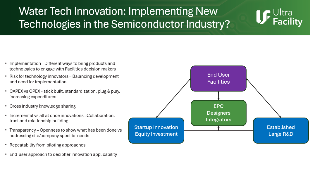
From Bulk Supply to Precision Treatment
A clear division of roles is emerging: public infrastructure provides baseline supply and resilience, while semiconductor manufacturers invest in advanced on-site treatment for high-purity water and recycling. This reflects the sector’s strict water quality requirements, which municipal systems alone cannot meet.
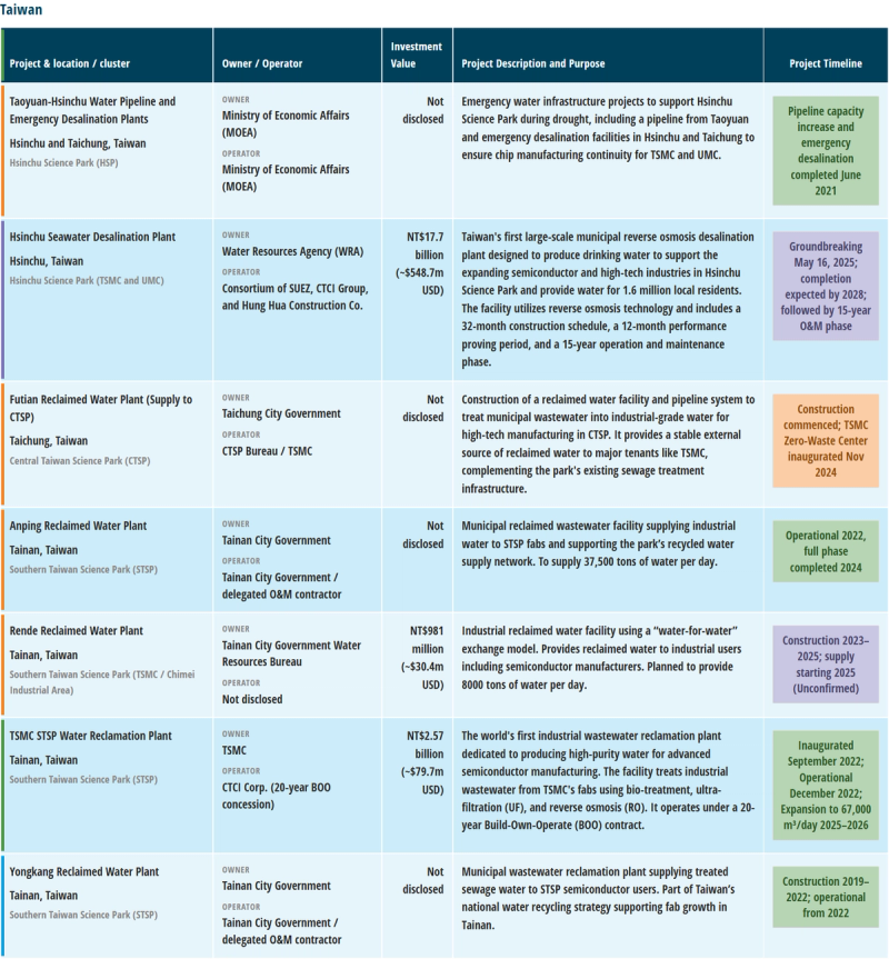
For example, the STSP Reclaimed Water Plant in Southern Taiwan Science Park treats semiconductor wastewater and supplies reclaimed water to TSMC fabs. As one of the first examples of UPW recycling, it helps reduce reliance on municipal sources after recent droughts. The system is supported by two city-operated plants, Yongkang and Anping, which supply water that is further treated and quality-checked at STSP before use.
Hybrid Financing Models for Water Infrastructure
A key trend is the use of hybrid financing and delivery models. In Taiwan and South Korea, projects are often structured as public-private partnerships, long-term offtake agreements or water exchange mechanisms, where governments and utilities fund infrastructure while semiconductor companies act as anchor customers to secure demand.
For example, the NT$17.7 billion ($548.7m USD) Hsinchu Seawater Desalination Plant is being delivered by Taiwan’s Water Resources Agency with partners including SUEZ, CTCI and Hung Hua under a 15-year O&M agreement. Similarly, the Rende Reclaimed Water Plant in Tainan operates under a water exchange model, supplying reclaimed municipal water to industry through agreements between the city government, national authorities and companies such as TSMC.
State-Driven Infrastructure in Emerging Semiconductor Clusters
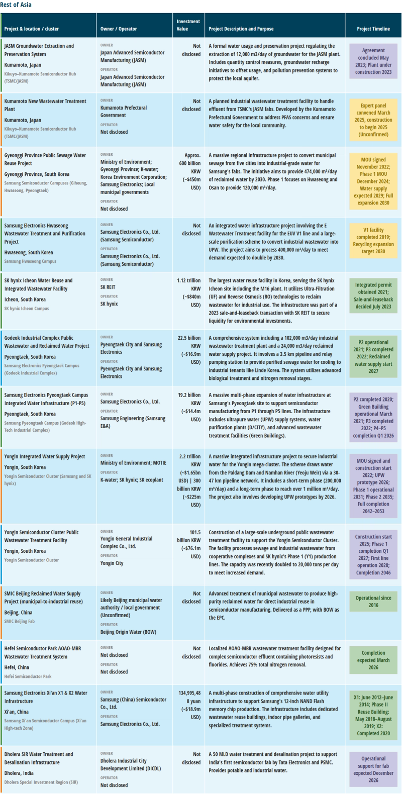
In China, large fabs such as SMIC typically build their own UPW and wastewater systems onsite, using private, invite-only EPC or EPC-O&M tenders, resulting in limited public visibility. By contrast, medium-size and smaller fabs in industrial parks (e.g. Shanghai Lingang, Hefei High-Tech Zone) rely on the park for raw water and basic sewage treatment but must pre-treat toxic and chemical wastewater to meet indirect discharge standards before entering municipal systems.
There is a clear shift toward more advanced onsite treatment, including ZLD, ammonia removal and membrane technologies, driven by strict regional water quotas and the need to increase reuse. This has also led to a small number of municipal-to-industrial reuse projects under BOT/PPP models. For example, Beijing Origin Water has supplied 5,000 m³/d of high-purity reclaimed water to SMIC Beijing since 2016.
However, full ZLD is not the dominant approach. In environmentally sensitive regions such as the Taihu Lake Basin (Wuxi, Jiangsu), stricter discharge standards push fabs toward minimal liquid discharge (MLD) as a more cost-effective alternative.
Public Pressure Influencing Infrastructure Development
In some markets, infrastructure is also being shaped by environmental and social pressures. In Kumamoto, Japan, local governments are planning a new wastewater treatment facility specially designed for semiconductor wastewater, in response to water quality concerns as semiconductor activity expands.
In Yongin, South Korea, local opposition over freshwater use delayed approvals for the SK Hynix cluster. In response, SK Hynix signed a 2022 MOU supporting the Yongin Integrated Water Supply Project, committing around KRW 300 billion (230 million USD) toward pipeline construction, alongside a planned government investment of KRW 2.2 trillion (1.46 billion USD) through 2035.
State infrastructure support for India’s emerging semiconductor landscape
India is taking a pre-emptive approach, investing in water infrastructure alongside early-stage fab development to attract manufacturing. The Dholera Special Investment Region (SIR), where Tata Electronics and PSMC are developing the country’s first semiconductor fab, includes a 50 MLD (50,000 m³/day) water treatment and desalination system designed to provide reliable industrial water supply to the emerging cluster.
See our previous article on US water utility projects:
Semiconductor in numbers: Water utility investments behind US mega-fab projectsShare this insight